Surface-Mount Construction
Surface-Mount Technology
This picture shows the future.
Well, no, it doesn't.
It shows the present.
Surface-mount technology has been the current state of
the art for some time now.
Traditional "through-hole" electronic components are usually
much larger than necessary, and they are rapidly becoming
much more expensive than necessary.
What's more, they are becoming less available!
It's time to move to the current technology and use
surface-mount technology (SMT)!
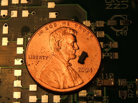
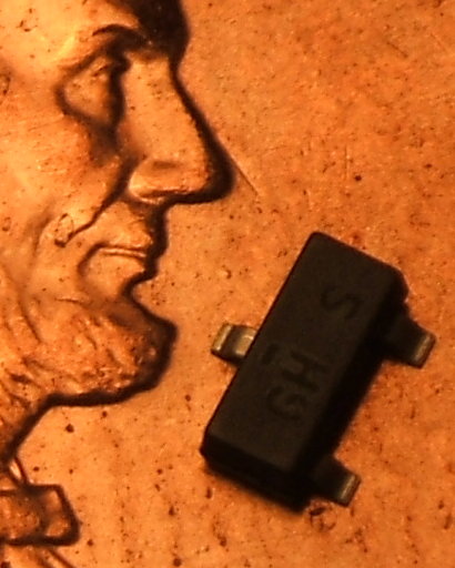
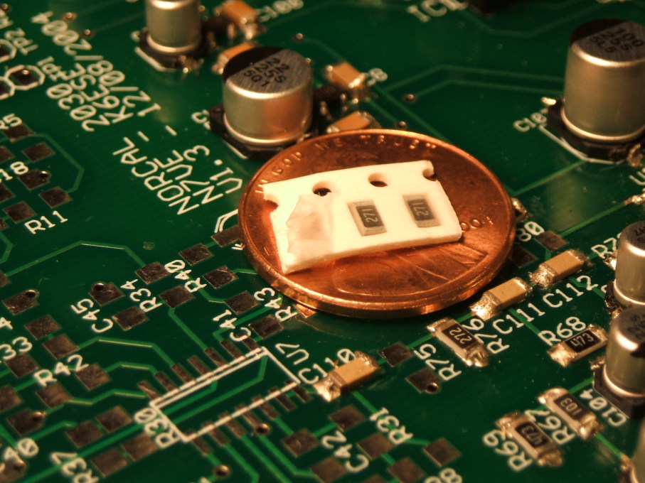
But aren't these components awfully difficult to use? Look at those tiny tab contacts on that three-port device! They're much smaller than Lincoln's bow tie!
Well, yes, that type of component was the one that I found the most difficult to solder into place in this project. But most of the components are relatively larger rectangular two-contact slabs.
Notice the bright square contact pads on the board. Those will be used for the much more numerous larger two-terminal components such as resistors, capacitors, inductors and diodes.
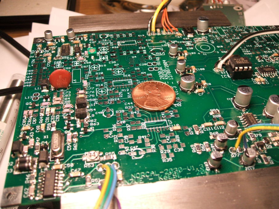
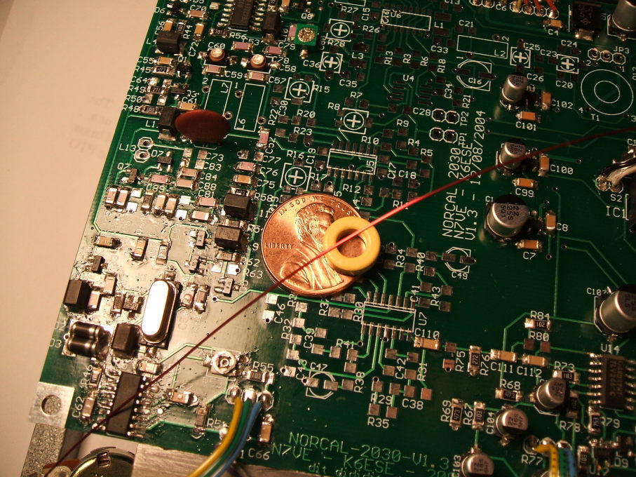
See one of those two-terminal components just below and to the right of the date on the coin. It's a capacitor in a location marked as C110.
Here is a multi-generation family portrait!
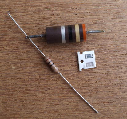
At top — A two-watt carbon composition resistor, the type commonly used in "hollow-state" electronics. That is, vacuum tubes and their high plate voltages. Look at the diameter of those high-current leads! Its color code is: Red, White, Black, Silver, so:
Red = 2
White = 9
Black = ×100 = ×1
Silver = ±10%
So, its value is 29Ω, ±10%.
At lower left — A quarter-watt carbon film resistor, toward the smaller end of the "through-hole" design but much larger than surface-mount. Its color code is: Brown, Black, Black, Gold, so:
Brown = 1
Black = 0
Black = ×100 = ×1
Gold = ±5%
So, its value is 10Ω, ±5%.
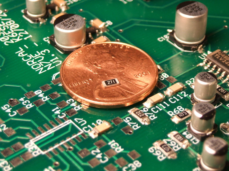
At lower right — A surface-mount resistor in a short piece cut from a long paper tape. What's its value? Let's look closer, see the picture below.
Here is a close look at that piece of SMT dispensing tape. The tape itself is thin cardboard with rectangular windows for the components and round holes for the feed system. Plastic film seals both sides, keeping the components in place until they are pushed out and placed on the circuit board.
Notice that this component is labeled 472. That's two value digits followed by a power of ten multiplier. This also happens to be a resistor, so its value is:
47 × 102 = 4700Ω
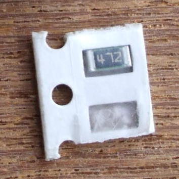
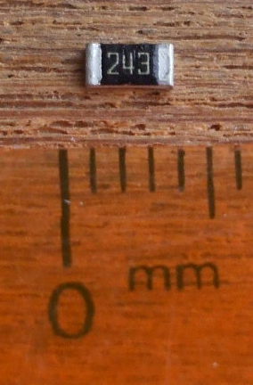
The second picture shows another resistor of the same size and design removed from its tape. It is labeled as "243", so 24kΩ.
The resistors above are size 1206 components,
a size specification indicating approximate dimensions
in hundredths of an inch.
1206 means a size of 0.126" × 0.063".
1206 specifies approximate dimensions because the real standard is metric. 1206 is the same as 3216 metric, indicating dimensions of 3.2 mm × 1.6 mm.
1206/3216 resistors are rated for quarter-watt power dissipation.
Here is that SOT-23 transistor package again, a little larger this time. The recommended circuit board lead pattern specifies SOT-23 pads just 1.25 mm × 0.6 mm.
You are going to need a soldering iron with a fine tip and some small diameter solder. NorCal included more than enough solder in the kit.
I decided to make this a lead-free build,
using Qualitek LF217 Sn/Ag/Cu solder in 0.032" (0.8 mm) diameter:
Silver: 3.8-4.2%
Copper: 0.3-0.7%
Tin: balance
It is very important to make up your mind about whether to use lead-tin solder or not, and then stick to that plan when making any later modifications or repairs. Lead-free solder alloys have higher melting points than Pb/Sn, and a mix of the two will lead to mysterious problems with cold solder joints.
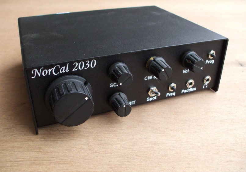
The Norcal 2030 HF QRP Transceiver
The NorCal 2030 or NC2030 is a nice HF QRP transceiver designed by Dan Tayloe, N7VE. It is an I/Q (or quadrature) direct conversion transceiver.
A stable local oscillator signal is produced by mixing a crystal oscillator of about 13 MHz with a PTO, or permeability-tuned oscillator, running at 3 MHz. A PTO is tuned by varying the inductance of an inductor in an L-C circuit — this is accomplished by threading a brass rod into a solenoidal inductor. The tuning knob simply threads slightly out of and back into the front panel! The tuning is a little less than 10 kHz per turn, so tuning is nice and gentle.
The 13.1 MHz crystal and 3 MHz PTO signals are mixed, producing 16.1 and 10.1 MHz outputs. The 10.1 MHz output is selected by a filter.
That 10.1 MHz oscillator signal generates an in-phase and quadrature (or I and Q) signal pair — that is, two signals identical other than a 90° phase shift. Some designs run the input oscillator at four times the desired output frequency and generate the I/Q signals with a simple digital circuit, click here to see an example of that. The NorCal 2030 uses a C-L-C phasing section to save power.
The quadrature detection is done with an SN743253 FET multiplexer / demultiplexer — it operates by switching rather than analog multiplication.
The quadrature outputs are amplified, combined through a 90° phase delay network, sent through filters and a further preamp stage, passed through a Maxim MAX7427 variable SCAF (switched-capacitor audio filter), and finally amplified to drive headphones.
A kit from NorCal, the Northern California QRP Club, included all parts, including a nice case and about 400 1206-size SMT components. The kit is no longer available, but the NorCal site still has lots of information about it.
It could be built for either the 20m or 30m band, depending on a few component choices and toroid winding details. I chose to build mine for 30m, as I already had a QRP transceiver for 20m.
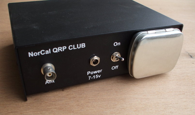
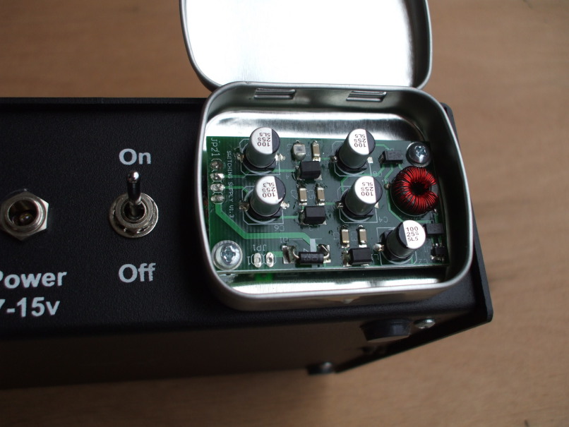
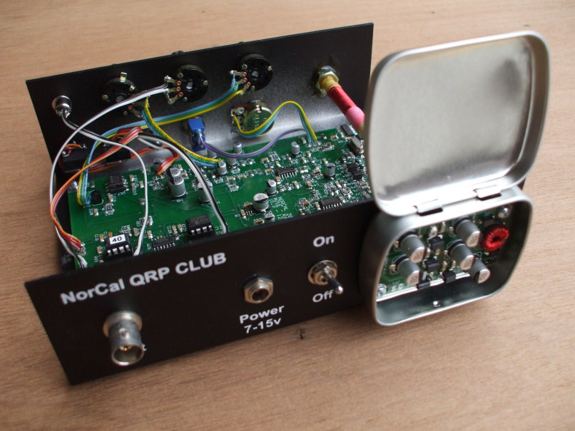
The radio requires just very nominal 12 volt DC supply, anything from 7 to 15 volts should work. The input DC voltage runs a small switching power supply to generate stable and clean 5.5V and 3.3V outputs. The switching supply (based on more Maxim chips) is in a small aluminum snap-lid case on the exterior of the main case, to keep the switching noise out of the radio.
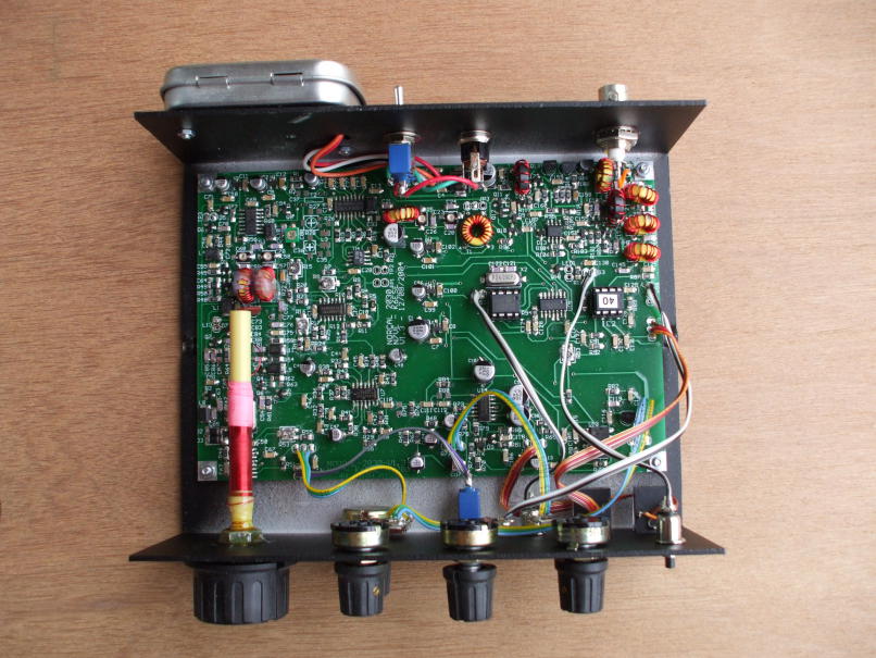
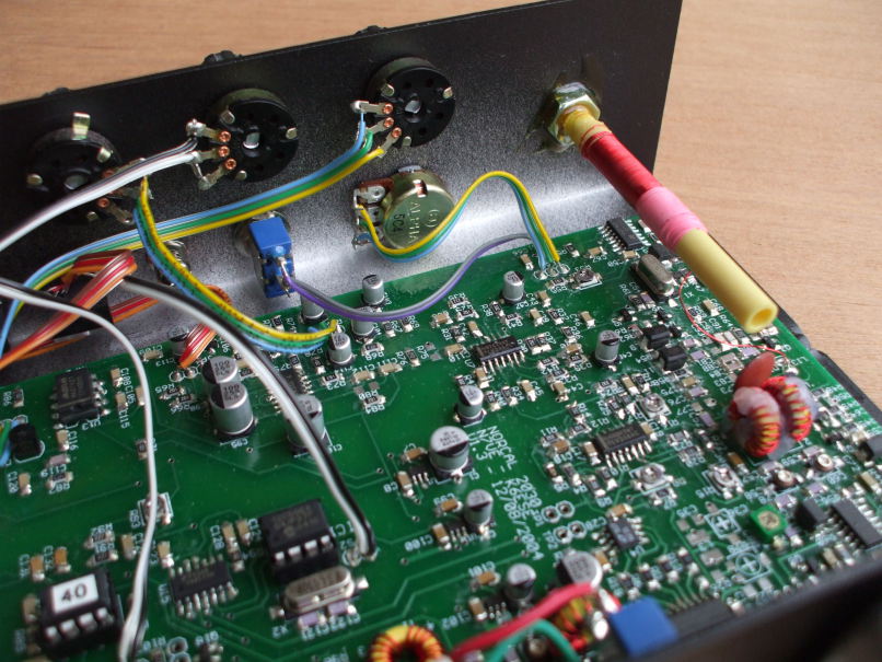
Here is the radio with the case cover removed. The PTO tuning knob is at the left. Rotating it slightly changes the position of a brass threaded rod within the inductor extending back into the case from the front panel. The antenna connector is diagonally opposite. The three toroids of the low-pass filter are lined up to its lower right. ro
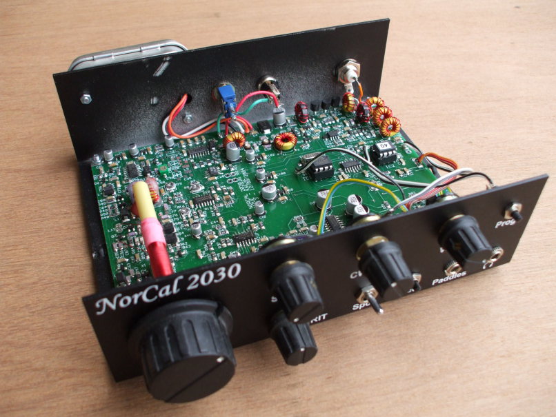
Small sections of ribbon cable connect the various controls for volume, CW speed (a keyer is included), the SCAF filter, and RIT (receiver incremental tuning, adjusting the transmit / receive offset), plus switches for the keyer and the frequency annunciator.
The frequency annunciator is a frequency counter chip. When you press that button, it tells you the current frequency by inserting Morse code into the headphone audio. Really — it tells you the frequency using CW!
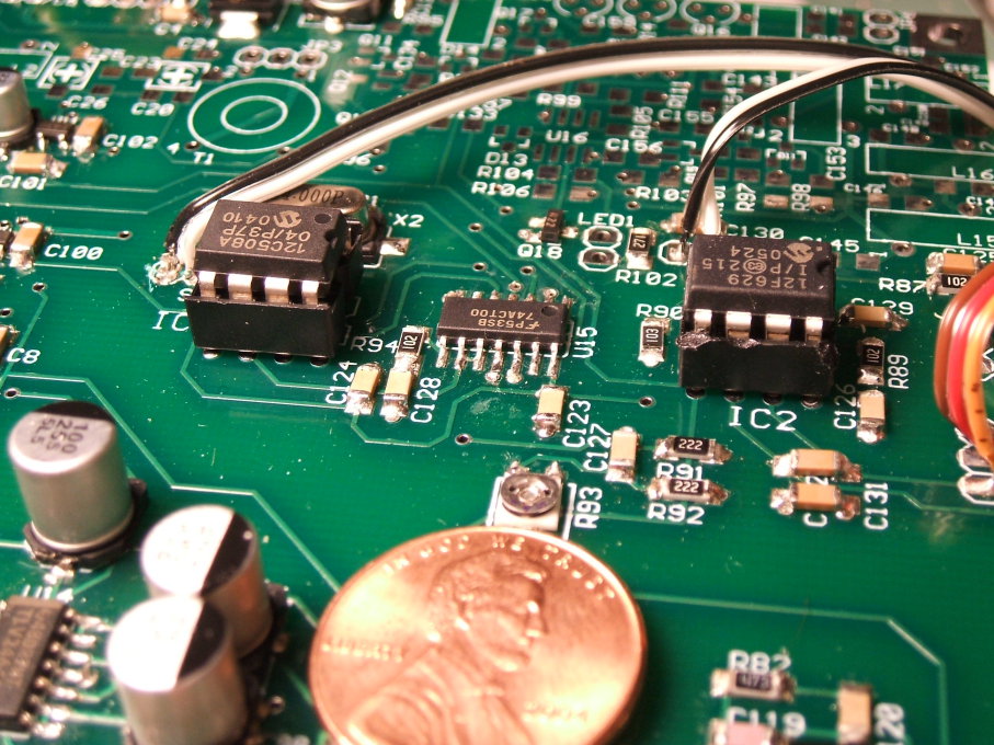
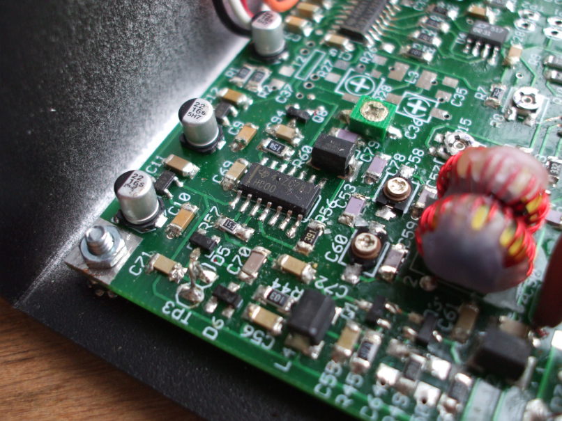
Three integrated circuits are in the relatively large DIP package — the SCAF audio filter, the keyer, and the frequency annunciator. Two of them are visible at right, all three of them below. The other integrated circuits are all surface-mount, in SOIC or Small-Outline Integrated Circuit packages with 1.27 mm lead spacing.
Building The Norcal 2030
Let's get started building the NorCal 2030! You're going to need something to hold the circuit board. I used a small metal-working vise from Harbor Freight, although a dedicated circuit board holder would have been nice.
You will also need a good source of light, and a magnifier on some sort of adjustable mount, so that you can easily do some of your work while looking through the magnifier. I used a simple goosenecked desk lamp and a small magnifier on a stand. An integrated magnifier and lamp would have been nice, but I didn't find it necessary.
The instructions were clearly written and illustrated, you download a PDF file containing the 128-page manual. But at least as importantly, the assembly process was well designed. You build a small section at a time, and then test your work so far. It starts with the power supply, then moves to small sections on the main board.
You will need a fine tipped soldering iron and a means of keeping it clean. I used a wet cloth pad in a glass ashtray.
Here are three integrated circuits. The comparatively very large 8-pin DIP chips at left and right are IC1 and IC2, PICs programmed as the CW frequency annunciator and the key, respectively. The SOIC (or Small-Outline Integrated Circuit) package in between is U15, a simple 74ACT00 quad NAND gate used by the frequency annunciator. Its leads are spaced at just 1.27 mm, half that of DIP.
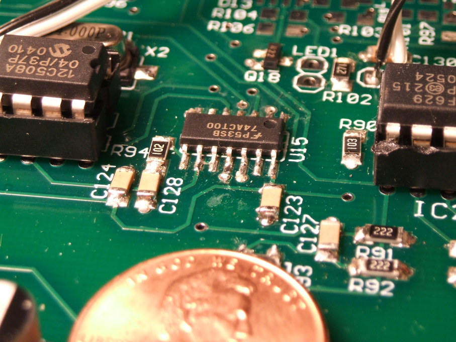
Below you see IC1, U15, and IC2 in closer detail. The SOIC chips are not at all difficult to solder as long as you have a clean fine tipped iron!
Start by very lightly tinning one of the corner pads. Don't apply solder to the pad. Just have a little solder on the iron tip itself and hold it on the pad briefly. When the pad is heated, a little of the solder will flow from the iron onto the pad and form a very thin film.
Carefully check the part number. NorCal had heat-sealed some plastic bags into multiple chambers. Once you're certain you have found the right part, cut that bag section open and extract the part.
Be very certain that you have the chip correctly placed and oriented. Hold it in place with a small wooden probe. I find wooden chopsticks very useful for this! Use the ones that are relatively pointed, not blunt. If your local Asian restaurants only give you the blunt ones, sharpen yours with a file. Touch the hot iron tip to the pad-pin joint long enough to liquify the thin film of solder. Surface tension will pull it through mating surface.
Remove the iron while still holding the chip in place with the chopstick.
The chip is only held in place by one very lightly soldered pin. Now is your last chance to catch an error! Make certain that you have the correct part, and that it is in the correct orientation.
Once you are certain, touch the iron to the diagonally opposite pin, and then touch the solder to the pad. Surface tension will pull the molten solder through the surface interface.
Amazon B06XZ31W3M
Go back to the first pin, heat it and give it a touch of solder.
Now go around and carefully solder all the other pins.
Once you think you are done, very carefully inspect your work with good light and magnification. Make certain that every pin is soldered to its pad, but that there are no solder bridges between pads. If you do have a solder bridge, you can probably fix it pretty easily. Put the iron on the bridge itself, melting the solder on both contacts. Then draw the iron tip away from the chip onto the green board surface. Surface tension will probably solve your problem.
If not, you probably have too much solder! Place some solder wick on the row of pins and heat the contacts through that wick. The excess solder should be drawn into the wick and you can clean things up. Don't add so much solder the next time.
One of the two component types that gave me the most trouble was the SOT-23 three-terminal device, transistors and diode pairs, because their contact tabs were so small. See two of these above, next to the large electrolytic capacitors in metal cans.
The other troublesome component was, surprisingly, one of the largest ones. The electrolytic capacitors were difficult to solder manually, because they are really designed for reheat flow soldering, where a machine has precisely placed solder paste on the pads and then placed components on those pads. Their contacts are tucked underneath.
The trick with them is to very lightly tin both pads, hold the capacitor in place, and heat the contact and the edge of the pad from the side. The only complaint I had with the entire design was that I wished that the board's pads for the electrolytic capacitors could have been a little wider than absolutely needed, making it easier to heat the pad and contact without melting the plastic base of the capacitor.
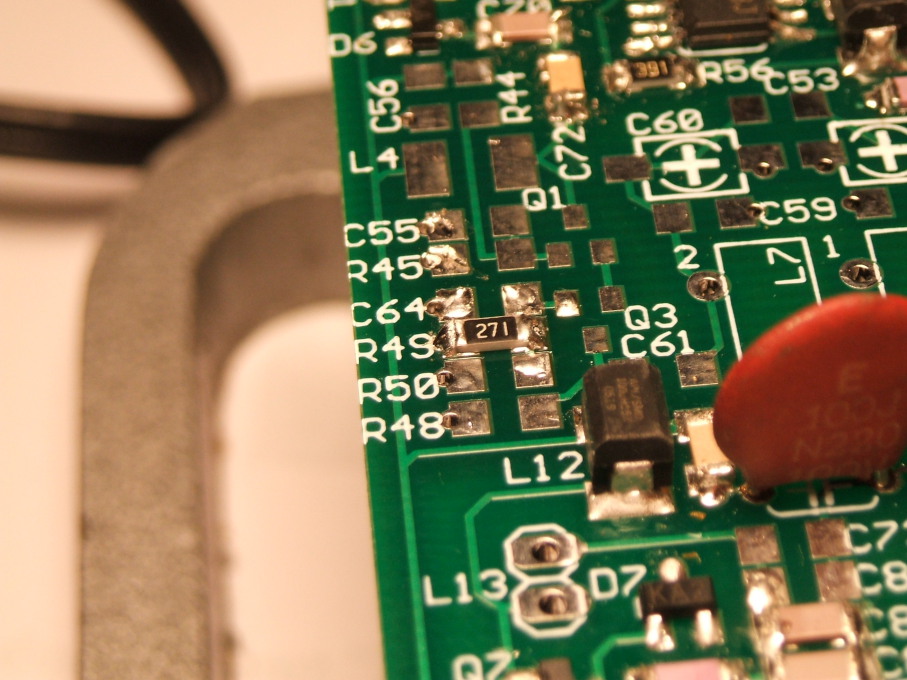
OK, let's install a 270Ω resistor. Let's get the tape fragment out of the bag compartment, and verify that its resistors say 271. The resistors in the kit were all labeled. The capacitors generally were not, and therefore required extreme care to only remove one at a time and not lose track of what you were doing.
Yes, this says 271, so remove just one by pulling the clear plastic tape back to open one more window in the tape.
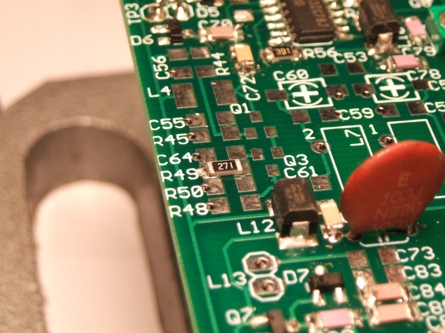
In this section I will be installing, among other components, that row of six components running down the edge of the board — C55 down through R48. This 270Ω resistor will be R49.
I have very lightly tinned one pad for each of those components, the pad nearest the board edge for each one. I have held the resistor in place, heated that outer pad, and the solder has wicked into the joint between the pad and resistor, and wicked slightly up the exterior face.
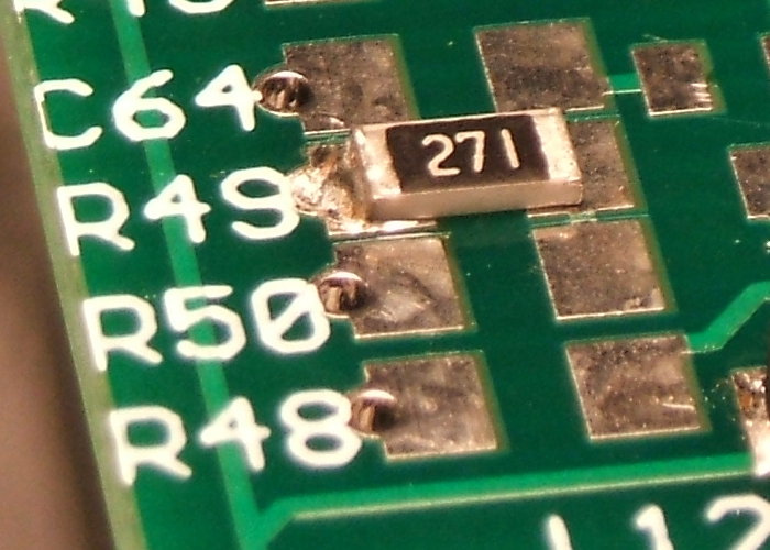
The second image shows a close-up of the partially installed 270Ω R49 resistor.
You can see through-holes for the pads nearest the board edge for components C64, R49, R58, and R48. The one for R49 is filled with solder now. Those through-holes are tinned and connect those pads to a ground plane on the underside of the board.
Notice how the solder has wicked itself in between the pad and resistor, and up the vertical face of its left end.
Also notice that the right end of the resistor is simply resting on its pad. That pad was not tinned, so the resistor can be mounted flush against the board by heating just the pad. That's good — it means that the resistor itself and its solder joints will be under no stress once both pads are soldered.
Now I have heated the other pad for that resistor and applied some solder. Next it will be time to go back and re-heat that first end.
In the process of doing this, I got some solder onto the inward pads for both C64 and R50. I need to clean that up before continuing.
This was early in the process, before I got a little better and cleaner at doing this.
Notice the two triangles of small pads marked Q1 and Q3. Those are two of those small SOT-23 packages, and they have to go on soon.
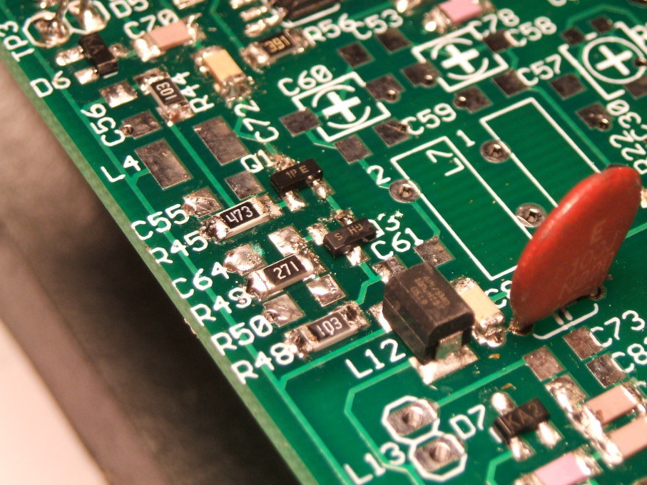
I have added two more relatively large 1206 resistors, R45 and R48, and I have also added those two troublesome transistors. Also, the similary packaged dual diode unit, D7, near the bottom of the picture.
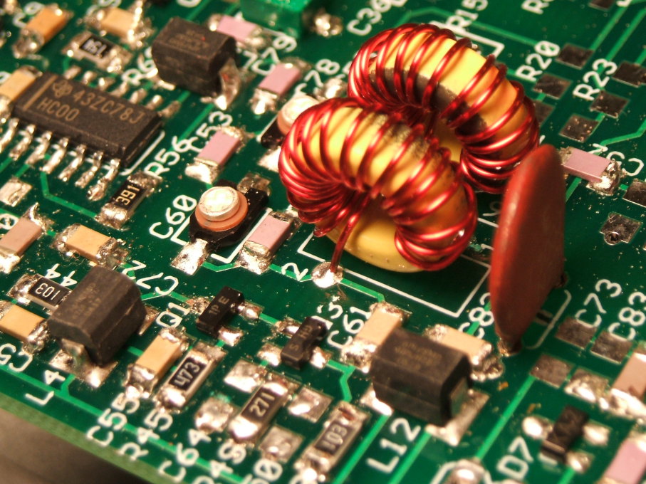
Notice the bulky surface-mount inductor, L12. Its contacts are tucked under. But their design exposes a relatively large vertical end face, allowing me to heat the lead, and the circuit board's design provides broad pads so I can easily heat the pad at the same time. Components like that are quite easy to install.
A design exception was made for the large through-hole disc capacitor seen here, as it provides power supply bypassing critical for keeping the PTO stable.
Now it's time to wind some inductors!
Every time the wire passes through the center makes for one turn. Some people mistakenly count the number of loops around the exterior of the toroid, making all their toroids have one turn too many and be a little high in inductance.
It's important to space the turns evenly around about 300° of the toroid. That is, the turns should occupy about five-sixths of the toroid, and the spaces between adjacent turns should be equal.
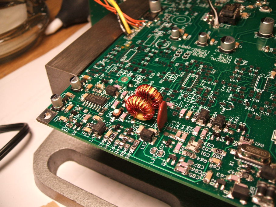
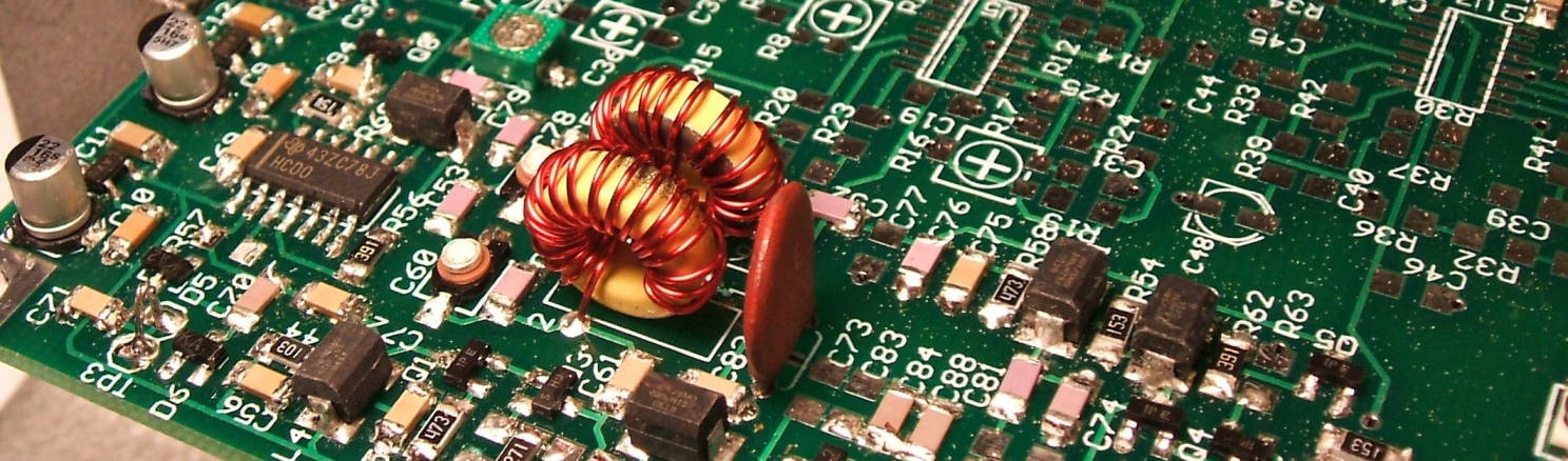
Here are two toroids wound and soldered into place.
These are L6 and L7, parts of the tuned low-pass filter selecting the desired output product of the mixer combining the crystal oscillator and PTO signals to generate the 10.1 MHz oscillator.
Capacitor C60, visible immediately to their left, and C58, only partly visible behind the nearest toroid, will be adjusted to tune this filter.
Finally!
All the components have been installed on the circuit board, the controls connected, and everything assembled into the case.
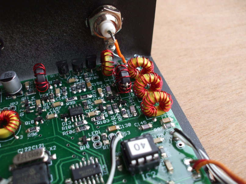
Here is the antenna port, with the three toroidal inductors and other components of the low-pass filter along the edge of the board.
The three BS170 MOSFET transistors making up the final power amplifier are lined up along the back edge of the board.
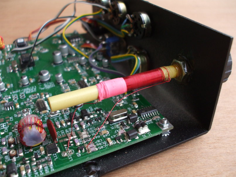
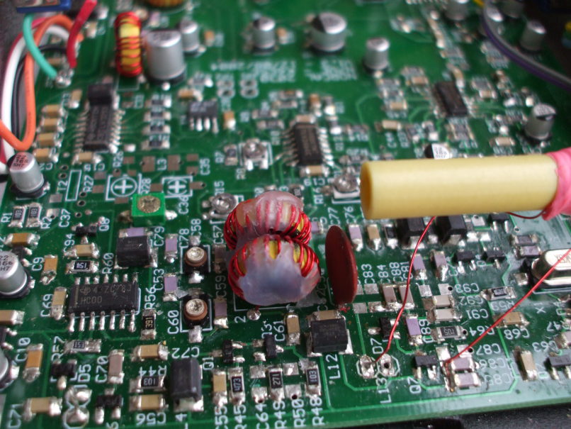
Above you can see the PTO tuned inductor. It is tuned by intentionally winding it with a couple of extra turns. Too much inductance, so a slightly low frequency. You then remove windings from the left end, under the pink teflon plumbing tape, removing a half-turn at a time.
Notice that some hot candle wax has been dripped onto those two toroids of the LO filter, to stabilize them and prevent microphonics — audible sounds or changes caused by mechanical vibrations or impulses changing their inductance, and thus their frequency response.
Here you see the fully populated board, the waxed inductors, and the adjusted end of the PTO inductor.
You can see here that many components are not used. Dan Tayloe did quite a bit of experimenting while developing the design, and not everything was needed in the final version.
The inductors have been waxed, capacitors C58 and C60 have been tuned, and many other adjustments have been made.
Here is a view looking in the opposite direction across the board. The SCAF chip is at the front of the board, at left here, tucked in underneath the front panel controls.
Now it's time to see what it can do!